
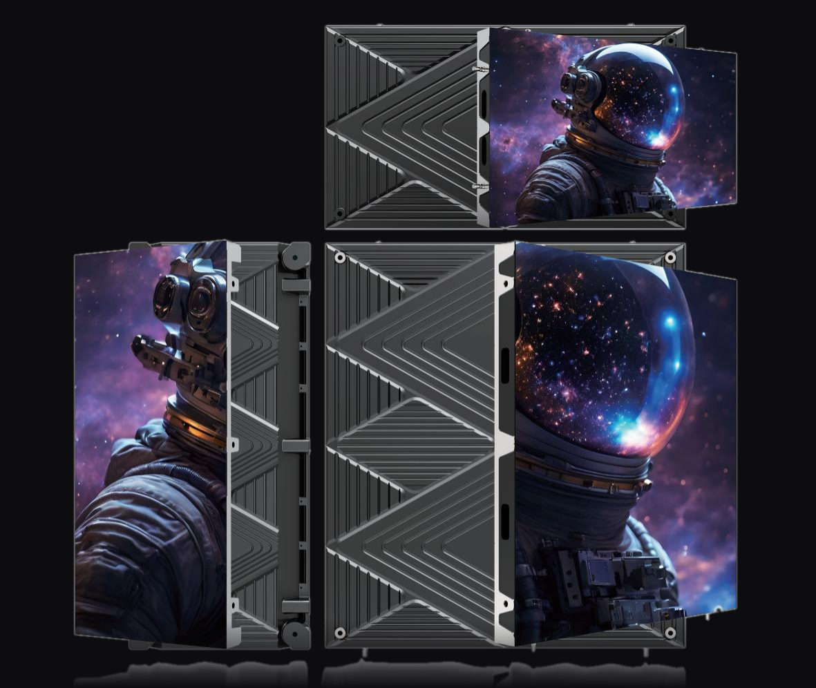
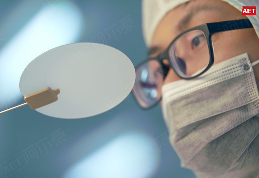
Red, green and blue light build the world we see, and behind those three colours sit completely different material science, process routes and industrial dynamics.
In 2026 the themes of strengthening and connecting the display supply chain remain central in China, and the deep restructuring of that chain is happening now. This new series walks the full journey from material to module, chip to screen.
Where Colour Comes From
Human vision depends on three kinds of photoreceptor in the retina, most sensitive to long, medium and short wavelengths — red, green and blue. The brain reconstructs every colour we perceive from the relative strength of those three signals.
That physiology sets the underlying logic for all modern display, from CRT to LCD, OLED to LED: mix three primaries in different proportions and simulate the colours of the natural world. For LED display it means we need semiconductor devices that emit each primary efficiently — and different colours place very different demands on the material. That is why the LED supply chain forks at its source.
Red: AlGaInP on Gallium Arsenide
Red light sits around 620 to 750 nanometres. Its emitting material is aluminium gallium indium phosphide, a quaternary compound semiconductor grown epitaxially on a gallium arsenide substrate.
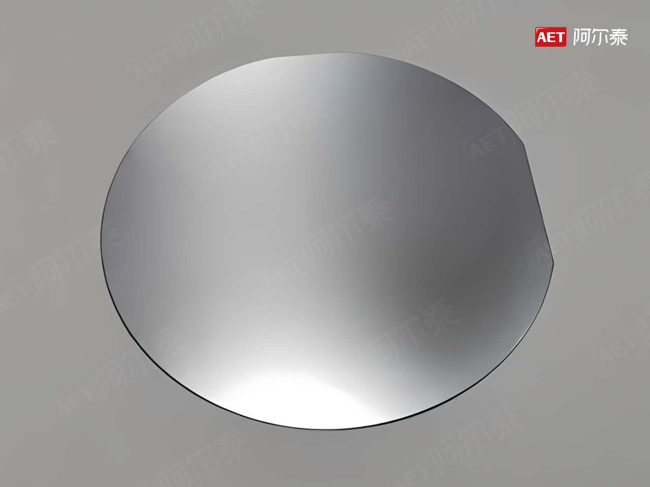
AlGaInP is used because in the red band it offers a unique combination of direct band gap, wavelength tunability, lattice matching and manufacturability at volume.
-
Substrate Gallium arsenide, typically 4 to 6 inch diameter.
-
Epitaxy Growth temperature around 700 to 800 degrees Celsius.
-
Structure Because GaAs absorbs light, red chips use a reflective structure that redirects downward emission upward, or a flip-chip structure, to raise extraction.
-
Trade-off The technology matured early, but substrate cost is high and wafer size is constrained.
Blue and Green: InGaN on Sapphire
Blue at 450 to 495 nanometres and green at 495 to 570 nanometres come from a different system: indium gallium nitride, grown on GaN or a heterogeneous substrate such as sapphire, silicon or silicon carbide.
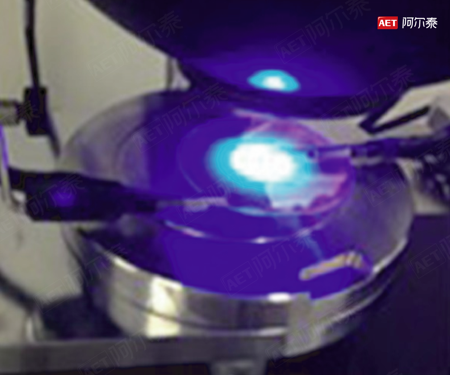
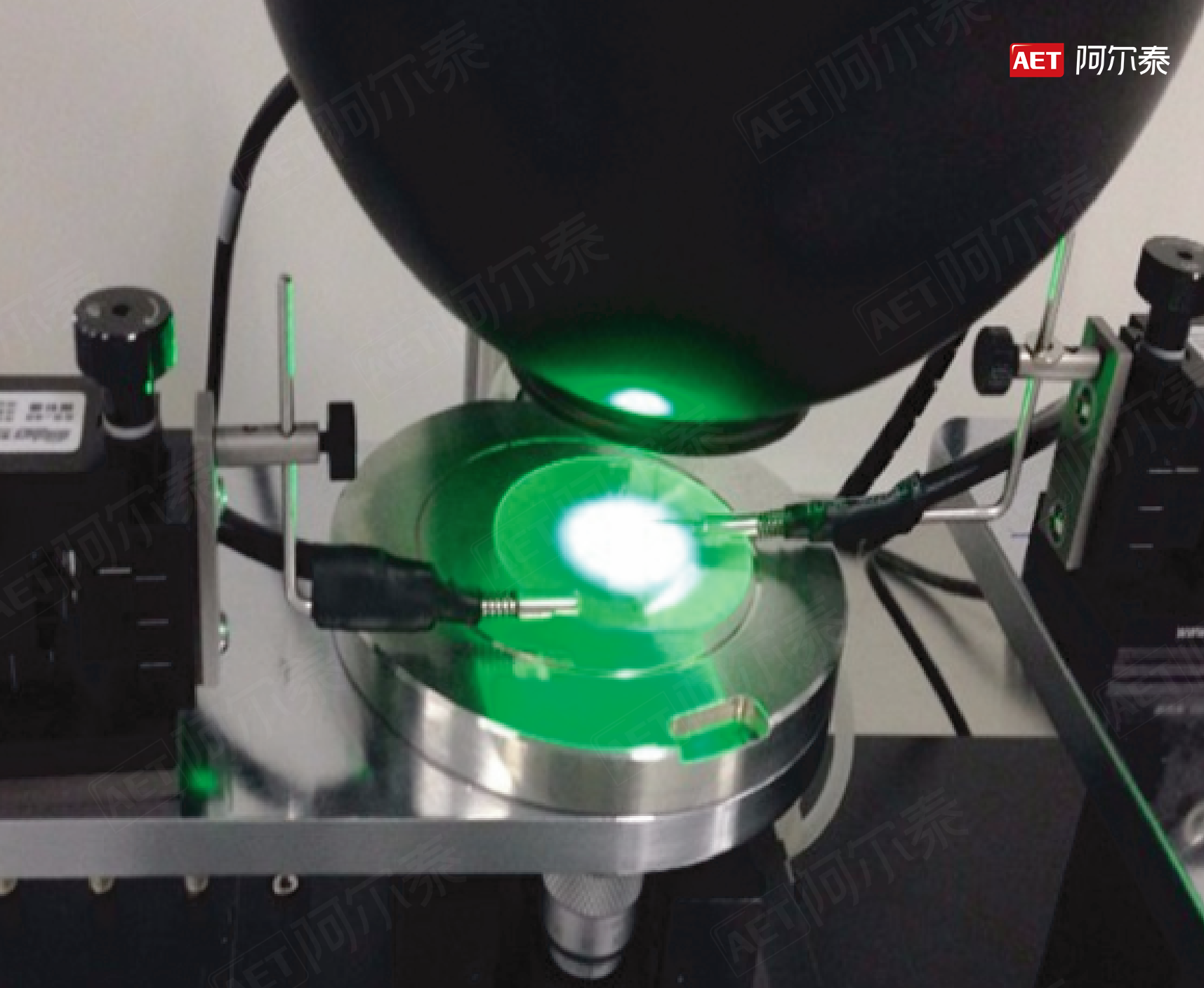
GaN-based material is the latecomer that made LED display possible. When Shuji Nakamura produced high-brightness blue LEDs on sapphire in 1993, full-colour LED display became feasible: without blue there is no complete spectrum to mix with red and green.
-
Substrate Sapphire is mainstream for transparency and cost, silicon carbide serves high-end work, and silicon is the cost-down direction.
-
Epitaxy Growth temperature of 1,000 to 1,200 degrees Celsius, a harder process.
-
Green gap Green has long trailed red and blue in efficiency, though the gap has narrowed in recent years.
-
Structure With a transparent substrate, chips can be built face-up or flip-chip.
The Deeper Reason: Semiconductor Generations
Behind these process differences is a deeper industrial logic: LED chips of different colours belong to different generations of semiconductor material.
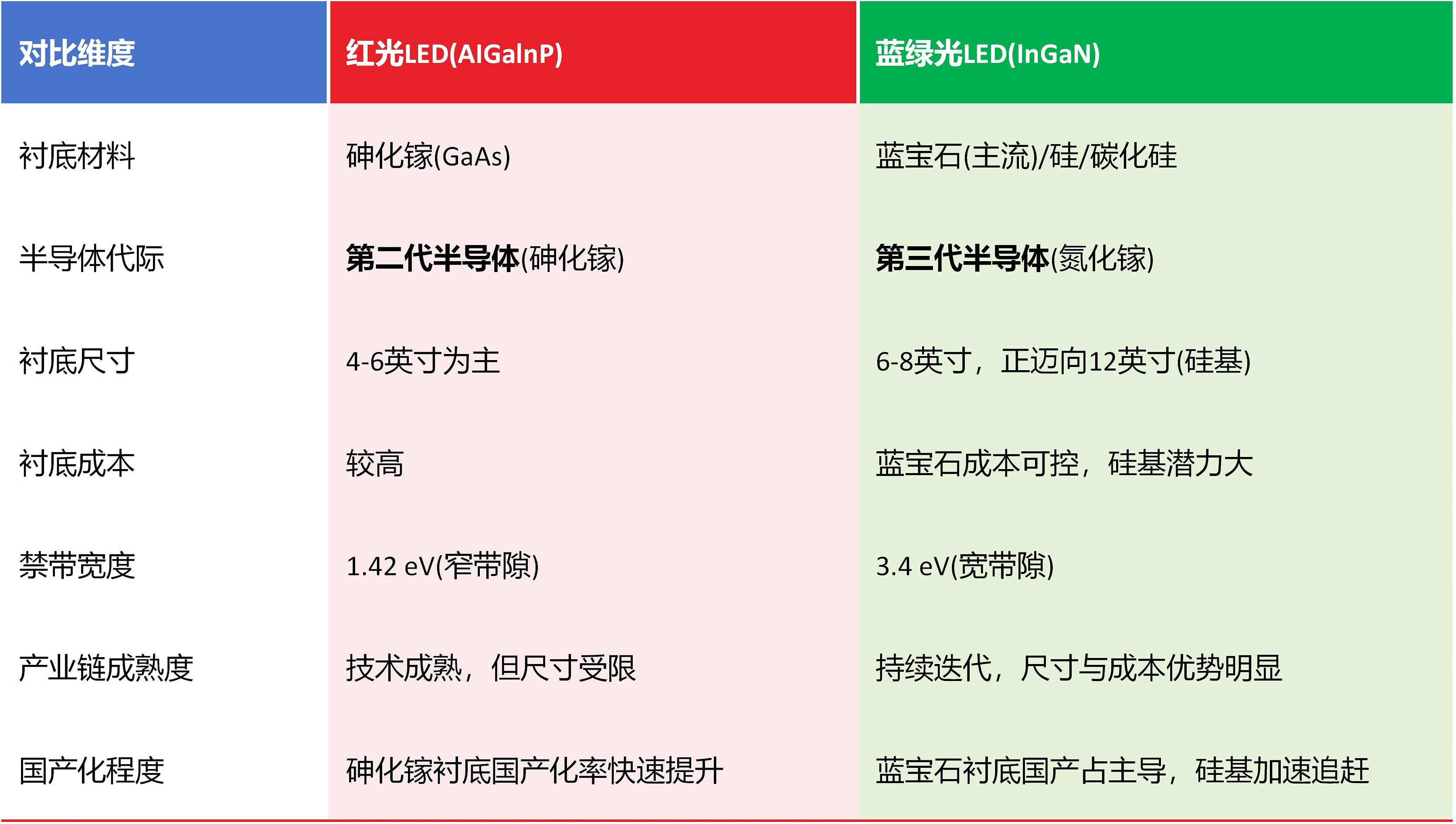
That generational split means the production equipment, process parameters and yield strategy for red chips and for blue-green chips are entirely different. It is why LED fabs are generally organised as a red line and a blue-green line — two parallel rivers that separate at the source.
Three Open Problems
Green efficiency. Among the three primaries, green has long been the laggard. In the InGaN system the growth window for high indium content is narrow, phase separation and defects appear easily, and internal quantum efficiency falls. Improved epi structures and chip designs have lifted green considerably, but a gap remains, and it directly limits the power-brightness balance of a full-colour screen.
Red substrate localisation. Gallium arsenide is a second-generation semiconductor material that was long imported. Domestic GaAs substrate capacity has expanded quickly and quality has improved, with localisation passing an important threshold — lowering red chip cost and improving supply security.
Micro LED full colour. How do you integrate millions of micron-scale red, green and blue chips on one backplane? This is fundamentally a heterogeneous integration problem between second and third generation materials. The conventional answer, transferring each colour separately onto a driver backplane by mass transfer, is complex, low-yield and expensive.
The routes under exploration all point the same way: from discrete primaries to integrated ones, from a fork between generations to a fusion of them. That is also the historic opportunity for the Chinese LED industry to move from following to leading.
Answering the Customer’s Questions
Understanding the physics, the generational split and the industrial fork makes these conversations easier.
Why is a red chip more expensive than a blue one? Because red uses a second-generation GaAs substrate, which costs more and comes in smaller wafers, and the flip-chip structure is more complex — while blue uses the third-generation GaN system with clear scale advantages.
Why is green LED efficiency low? It is an inherent challenge of the GaN system, where high-indium epitaxy is difficult. Technology has moved a long way, and high-end green products are now much better than they were.
Why is Micro LED so hard? Because it requires efficient integration and mass transfer of second-generation red and third-generation blue-green materials at micron scale — a systems problem across material, equipment and design, not only a process problem.
How far has import substitution come? GaAs substrate localisation is rising fast, sapphire for GaN is already domestically dominant, and GaN-on-silicon is catching up. A self-controlled supply chain is taking shape.
Where AET Sits
If the fork happens at the substrate and chip stage, that is exactly where AET has built its capability.
-
Red Volume production of 4 to 6 inch GaAs substrates for optoelectronics, supporting high-end red LED efficiency and reliability from the source.
-
Blue and green In-house patterned sapphire substrate technology, providing a high quality base for InGaN epitaxy and improving light extraction, consistency and yield.
-
Next generation Combined MOCVD and HVPE routes with 2 to 8 inch GaN single-crystal substrate production, 8-inch performance leading internationally, and in-house epitaxy for Mini and Micro LED chips across blue-green and red.
Because control starts at the source, AET can optimise quality from the point where light is generated: every chip from the same technical system and the same quality standard, every screen carrying a promise that runs from origin to terminal.
The generational contest between GaAs and GaN — technology, wafer size and localisation — is the subject of the next instalment.
The Full Supply Chain, Explained
This series decodes the LED industry from substrate to screen. Contact AET if you would like the complete set, or a briefing for your team.
Related Articles & Insights
AET Opens Global Recruitment Across R&D, Sales and Service
AET has opened a global recruitment round covering display research, engineering, overseas sales and field service.
Five Extremes: How AET Plans to Grow
Minimalist architecture, frontier technology, visual quality, fine pitch and fast service: the five directions AET has organised i...