
MIP, COB, QCOB, GOB, IMD, SMD. The acronyms are everywhere and they are not interchangeable. This is a working guide to what each route is, what it is good at, and which project should choose it.
The Direction of Travel
Before the individual technologies, one point of orientation: direct-view LED is moving irreversibly from discrete device mounting toward integrated panel-level packaging. The driver is the permanent demand for smaller pitch, higher reliability, lower maintenance cost and better image quality. Conventional routes are approaching physical limits, and the newer ones are reshaping the industry through integration.
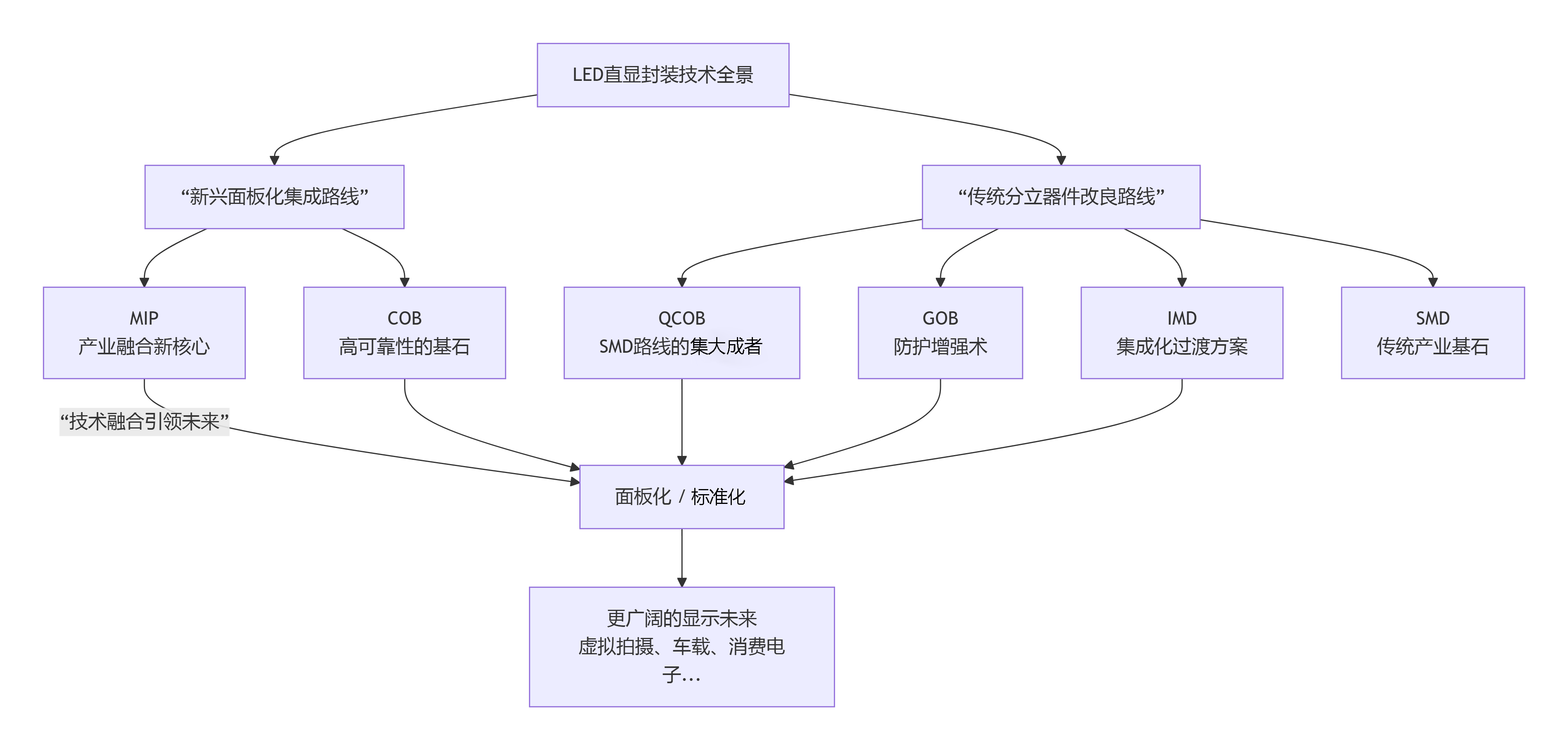
The technologies run in parallel rather than replacing one another in sequence.
MIP: The Industrialisation Route
MIP is the most watched variable in the market today, and in essence it is a route designed for industrialisation. Miniaturised LED chips are packaged first into independent, testable, binnable devices, then mounted onto the substrate.
Its value is that it bridges both ends: upstream it inherits the miniaturisation of Micro LED chips, downstream it is fully compatible with existing SMT equipment and process, which lowers the cost and the barrier of upgrading the chain.
Industry forecasts place MIP at the start of volume adoption now, with expansion expected around 2028 as cost and image quality carry it toward consumer markets.
AET’s recommendation: for projects that want ultra-fine pitch at a reasonable cost with high reliability and good image quality — premium commercial display, virtual production stages — MIP is currently the lowest-risk, smoothest step up.
COB: The Reliability Ceiling
COB packages LED chips directly onto the circuit board, which is the move from point to plane. The fully enclosed structure delivers reliability that discrete devices cannot: moisture, impact and dust problems are solved rather than mitigated.
Full flip-chip COB cost is falling quickly with process maturity and scale, and at P0.9 it is already competitive. It is standard in high-end command centres and broadcast studios, and is moving into premium meeting rooms and home cinema.
AET’s recommendation: where the requirement is 24/7 stability, maximum protection and long life, with budget available, full flip-chip COB is the flagship choice without argument.
QCOB: An Optical Upgrade on SMD
QCOB is a high-end optical improvement on the classic SMD route rather than a move to COB or chip integration. It takes the mature SMD device and adds AET’s high-temperature film lamination on a multilayer board, which lifts both image quality and reliability.
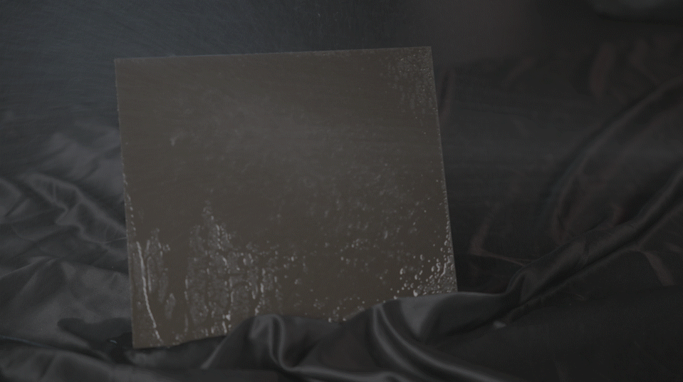
Visual comfort. Surface treatment softens the emitted light into a true surface source. Harsh reflection and glare are removed, resistance to ambient light is strong, and long viewing is comfortable.
Physical performance. Multilayer epoxy cured at high temperature makes the panel structure very stable and resistant to warping. The surface is warm to the touch, scratch resistant, non-mirror and resistant to marks, so it can be used directly as a touch surface.
AET’s recommendation: for premium retail, corporate showrooms, command centres and special environments where visual comfort, interaction and reliability matter, QCOB is the strong choice.
GOB: Armour for Difficult Sites
GOB is a targeted reinforcement rather than a new packaging method. A specially formulated room-temperature-cured transparent optical adhesive is applied over a finished SMD module.
The layer gives the panel strong physical and environmental protection — water, moisture, impact and dust — and converts a point source into a softer surface source, reducing moiré and improving how the screen photographs. The essential difference from QCOB is the curing temperature and the material system.
AET’s recommendation: GOB suits difficult environments. Outdoor advertising, rental stages and interactive showrooms subject to knocks all benefit from what amounts to insurance against maintenance risk.
IMD: The Transition Step
IMD, often called N-in-one packaging, integrates several pixels — 2 × 2 or 4 × 4 — into one package. It raises mounting efficiency, consistency and some protection for fine-pitch product, and balances the economics of SMD against some of the advantages of COB.
Above P1.0, particularly in cost-sensitive commercial projects, it remains competitive.
AET’s recommendation: for conventional meeting rooms and information publishing, IMD offers a good balance of cost and performance.
SMD: The Volume Route
SMD is the oldest and most mature route and remains the most widely used. Maturity, competitive cost and easy repair support a market that runs from outdoor screens to conventional indoor pitch.
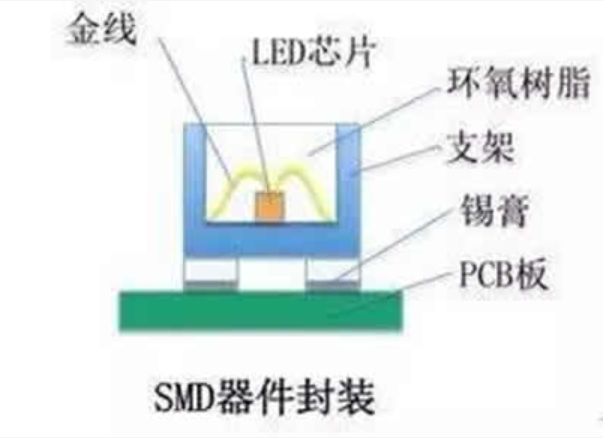
It has limits as pitch shrinks, but at P1.5 and above its maturity and economics keep it the mainstay. The existence of QCOB, GOB and IMD is itself evidence of how extensible the SMD route has proved.
AET’s recommendation: where the pitch requirement is not extreme (P2.0 and above), the budget is tight and the environment is standard, SMD is the most prudent commercial decision.
What Comes Next: Glass Substrates
The next chapter is not about one technology replacing another but about fusion, and the competition moves from packaging alone to packaging plus substrate material. Glass is central to that.
Glass offers extreme flatness, excellent thermal stability and compatibility with semiconductor processes, which makes it the leading candidate substrate for pitch below P0.4 and for consumer devices such as smart watches and AR glasses.
-
Glass plus MIP High-precision glass carries pre-packaged MIP devices for higher density and easier production at fine pitch.
-
Glass plus COB Chips are mass-transferred directly onto glass for maximum image quality and integration.
From SMD and its continuing refinements, through the panelisation wave led by COB and MIP, the history of LED packaging is a history of pursuing better image quality, higher reliability and a lower barrier to use.
Choosing a Packaging Route
AET supplies MIP, COB, QCOB and SMD products and will recommend a route against your pitch, environment and budget. Contact the team for a comparison for a specific project.
Related Articles & Insights
AET Opens Global Recruitment Across R&D, Sales and Service
AET has opened a global recruitment round covering display research, engineering, overseas sales and field service.
Five Extremes: How AET Plans to Grow
Minimalist architecture, frontier technology, visual quality, fine pitch and fast service: the five directions AET has organised i...