

Last time we looked at why red and blue-green light come from entirely different material systems. This time we go into the core of chip manufacturing: how a piece of substrate that emits nothing becomes thousands of individually emitting micron-scale chips.
The whole process is like building an extremely small, light-emitting house that has to be assembled with precision.
1. Substrate: the Foundation
Crystal bases such as sapphire and gallium arsenide provide the physical support for the entire chip.
Think of it as the flat, hard stone slab a house is built on. An uneven slab tilts the building; a dirty one ruins the lights. Substrate quality determines whether every later step succeeds.
2. Epitaxy: Growing the Emitting Layers
In MOCVD equipment, the N-type layer, the multiple quantum well emitting layer and the P-type layer are grown in sequence.
This is the house structure being grown layer by layer on the foundation. The special material in the middle is the floor that lights up when current flows. Without epitaxy, an LED is just an ordinary stone that will never emit.
3. Lithography: Drawing the Plans
Photoresist is applied, exposed and developed to define the micron-scale pattern for the following steps.
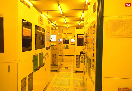
This is the construction drawing for the tiny house — where the windows go, where the wiring runs, where the lamps sit. Lithography sets how fine the circuit can be, and it must happen in a yellow-light cleanroom: ordinary light would destroy the pattern, the way daylight ruins a photographic negative.
4. Etching: Cutting the Shape
Dry or wet etching removes excess material to form steps and isolation regions.
Following the drawing, surplus material is cut away to leave the outline of the house, the circuit channels and the emitting area.
5. Electrodes: Fitting the Contacts
Metal electrodes for the P and N sides are deposited by vacuum evaporation.
Small metal contacts are placed at defined points, like fitting the positive and negative leads to a street lamp. Current enters here, and only here, so the lamp can light.
6. Face-Up or Flip Chip: Two Ways to Wire It
After passivation for protection, thinning for better heat transfer and dicing to split one wafer into thousands of chips, the LED chip is formed. Two structures exist depending on where the electrodes sit.
In a face-up build the lamp hangs below the ceiling with the wires in front of it, blocking light. In a flip-chip build the wiring is buried in the wall and the emitting face points straight out — all the light escapes, and the package is more robust.
7. Why AET Controls the Chain
A single small chip sits behind dozens of precision steps. Any deviation from substrate to epitaxy, lithography to etching, electrode to dicing affects the brightness, uniformity and lifetime of the finished screen.
Clients often ask what distinguishes one screen maker from another. AET’s answer is that it is one of the few companies in the industry that genuinely controls the chain from substrate and epitaxy onward — defining quality at the source and closing the loop vertically.
-
Not an assembler AET defines quality from the point where light is created, across the full supply chain.
-
One standard Every chip, every module and every screen comes from the same technical system and the same quality control standard.
-
Optimised backwards Chip performance can be tuned to the end application — a command centre or a studio — rather than to a generic specification.
From Chip to Screen
This is the first in a series on the LED supply chain. Contact AET for the full white paper or to discuss how chip-level control affects your project.
Related Articles & Insights
AET Opens Global Recruitment Across R&D, Sales and Service
AET has opened a global recruitment round covering display research, engineering, overseas sales and field service.
Five Extremes: How AET Plans to Grow
Minimalist architecture, frontier technology, visual quality, fine pitch and fast service: the five directions AET has organised i...