
Let the full chain become a guarantee the customer can rely on; let frontier technology become an experience the customer can see; let the product become a value engine the customer can actually use.
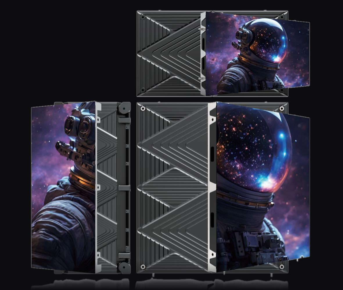
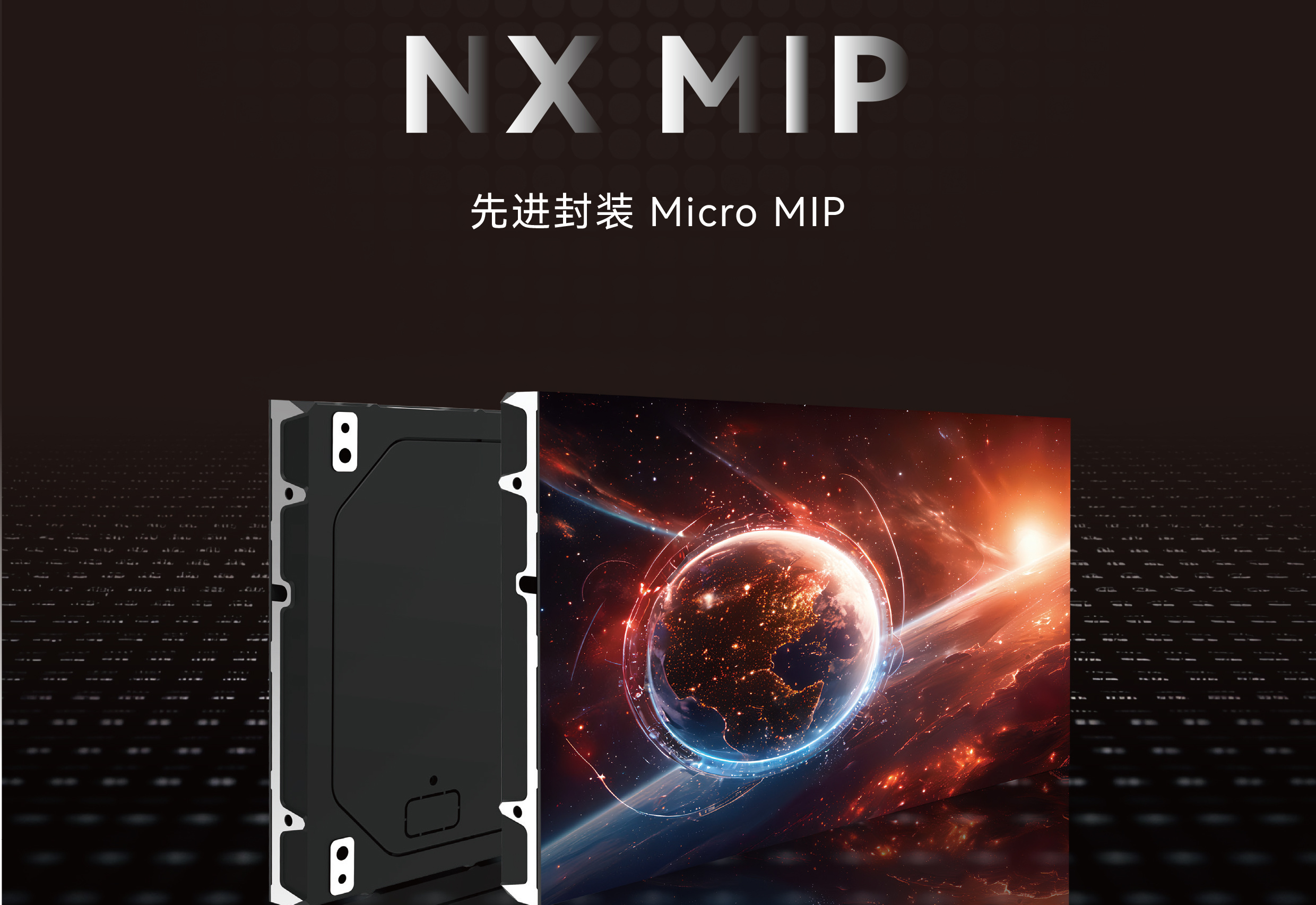
In 2026 AET formally launches the NX MIP series, covering both Micro-level and Mini-level MIP — a complete layout from extreme display to volume application.
To explain what the two products are worth, it helps to start with the platform they share.
What MIP Actually Is
MIP stands for Mini/Micro LED in Package. The idea is to package the Mini or Micro LED chip into an independent emitting unit first, then mount that unit onto the display module.
The essential difference from SMD and other approaches is that the centre of gravity moves from the lamp to the chip-level package. Put simply: SMD and IMD mount lamps onto a board, while MIP seals chips into a package.
In process terms MIP uses a flip chip with die bonding and die attach soldering, dropping the gold wire bonding step entirely, which makes the package more compact and more reliable. Three consequences follow.
-
Smaller and finer Supports ultra-fine pitch at P0.4 and below.
-
More reliable The package gives the chip structural protection and better resistance to stress.
-
Better light and colour MIP lamps can be colour-binned and mixed, giving better consistency across the module.
MIP is therefore not only a packaging upgrade but the bridge between today’s Mini LED industry and tomorrow’s Micro LED display.
At P0.6 and below, COG and COB approaches are constrained by mass-transfer yield, and volume production remains difficult. MIP uses advanced packaging — sapphire laser lift-off, mass transfer and RDL — to pre-form Micro LED chips into small packages, and is currently the leading route to stable Micro display production.
Mini-Level MIP: Volume, Reliability, Cost
Mini-level MIP uses flip Mini LED chips between 100 and 300 micrometres that still carry the sapphire substrate, packaged by die bonding. The technical difficulty sits in the front-end packaging step: how to seal Mini chips into MIP packages efficiently and stably.
-
Packaging efficiency One die-bond step transfers red, green and blue chips together, tripling throughput.
-
Lower process demand, higher yield The package is larger than the bare flip chip with wider pin and gap spacing, so PCB precision and die-attach accuracy requirements are lower.
-
Better uniformity Colour mixing at package level reduces the need for secondary binning of modules.
-
MIP plus GOB The display face reaches IP65, with the chip protected by the package for longer life.
-
Deployment Each unit ships in its own crate, modules are front-serviceable, wireless hard connection and hot swap are supported, and dual power and signal backup are optional.
-
Applications Meeting centres, commercial display and high-end retail at scale.
Micro-Level MIP: Extreme Fine Pitch
Below 100 micrometres, a Micro chip used directly on a display module runs into connection difficulty, low yield and poor reliability. Conventional wafer grinding and thinning on a sapphire carrier also becomes a bottleneck: cracking during grinding can push chip yield below 50%, which is not manufacturable. The answer is laser lift-off of the sapphire substrate.
Micro-level MIP therefore uses ultra-small Micro RGB chips with the sapphire substrate removed, achieving true chip-level packaging. It keeps the flip chip and die-bond structure and pre-packages micron-scale chips through laser lift-off, mass transfer and RDL into a structurally stable, larger package — simplifying back-end manufacturing and addressing repair, yield and line compatibility.
The hard problems sit in the back end: how to lift off sapphire efficiently, and how to break through Micro-chip mass transfer. With high chip cost and complex processing, the route is still ramping and not yet in mass adoption.
-
Optical performance With the substrate removed the chip is under 10 micrometres thick, viewing angle exceeds 170 degrees, and smaller RGB chip area and spacing improve colour mixing with no colour shift or blue-yellow fringing.
-
Contrast No gold wire to block light, smaller chips and a larger black area give contrast above 10,000:1.
-
Reliability No substrate and no bond wire, with pads and circuitry integrated, avoiding metal migration problems.
-
Specification P0.78 and P0.93, 3,840 to 7,680 Hz refresh, 13 to 16 bit greyscale.
-
Picture 1,200 nits, 12,000:1 contrast, fine detail and full colour.
-
Surface Nano-black treatment with a substrate-free emitting IC design gives a deep, clean black screen.
-
Protection 170-degree viewing, IP65 against water, dust and impact.
-
Service Wireless hard connection, hot swap, full front maintenance, optional dual backup, 2K to 8K and above, custom rear covers.
From the proven reliability of Mini-level MIP to the extreme display of Micro-level MIP, AET has used its integrated chip, packaging and application capability to bring both MIP lines to volume production and commercial deployment first.
The NX MIP Series Is Open for Business
Whether the priority is image quality, volume economics or a differentiated position, AET can configure an NX MIP specification around it. Contact the team for samples and roadmaps.
Related Articles & Insights
AET Opens Global Recruitment Across R&D, Sales and Service
AET has opened a global recruitment round covering display research, engineering, overseas sales and field service.
Five Extremes: How AET Plans to Grow
Minimalist architecture, frontier technology, visual quality, fine pitch and fast service: the five directions AET has organised i...