
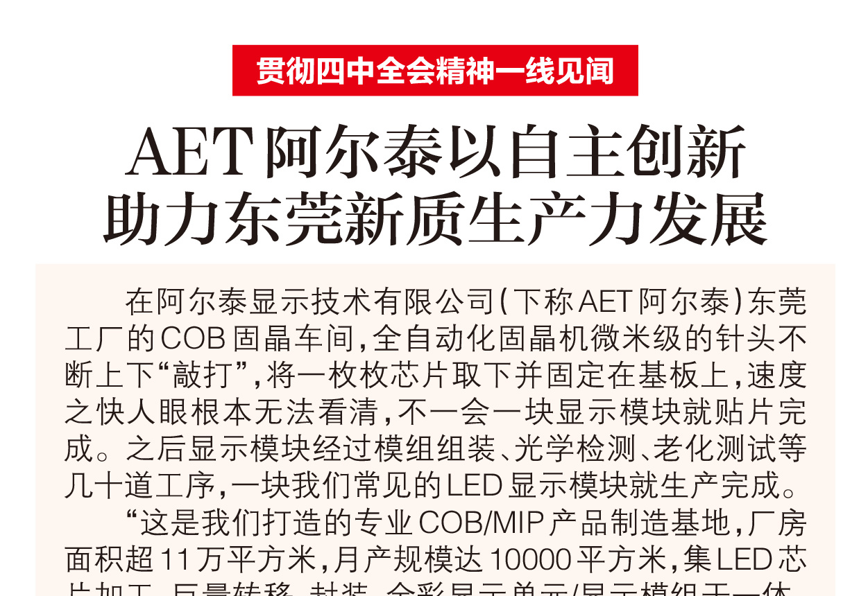
In the COB die-bonding workshop at AET’s Dongguan plant, automated bonders tap up and down at micron scale, picking chips and placing them on the substrate faster than the eye can follow. A display module is populated in moments, then passes through dozens of steps — module assembly, optical inspection, ageing — before it is finished.
A Dedicated COB and MIP Base
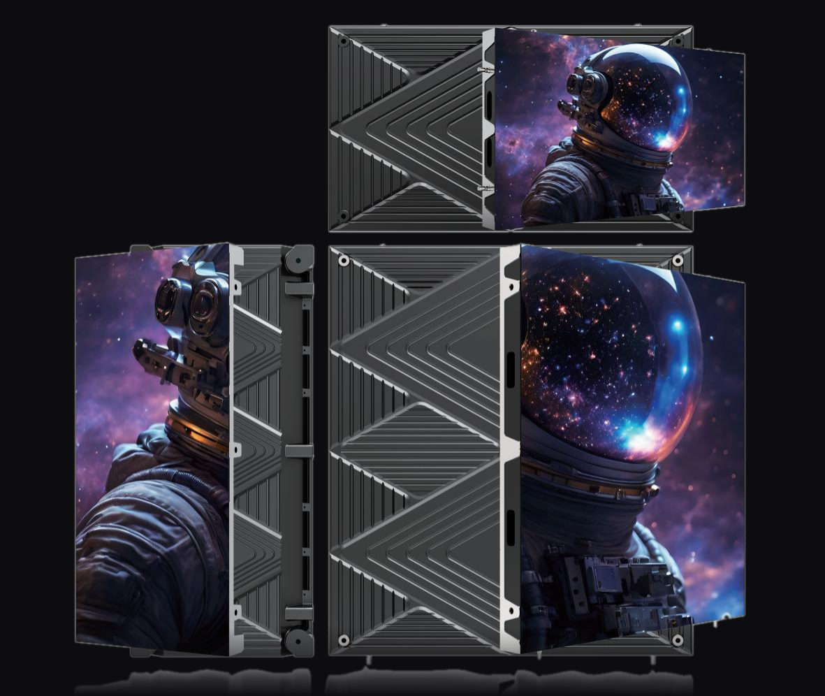
The site is purpose-built for COB and MIP: more than 110,000 m² of floor space and monthly output of 10,000 m², integrating LED chip processing, mass transfer, packaging and full-colour display units and modules in one chain, sized for the full Mini and Micro LED range.
General Manager Liang Hong describes an industry still moving quickly on materials and process, and a company that has kept raising research investment on top of its existing technical base — breaking new process ground, pushing standardisation and opening new markets.
Over RMB 2 Billion Into COB
AET was founded in 2016 and is a key subsidiary of Guangdong Guangda Group’s technology arm. It designs, develops and manufactures Mini and Micro LED products for commercial display, security monitoring, meeting, broadcast and entertainment, and home cinema.
Building a Mini LED display means combining semiconductor material, core chip, light source, high-density carrier board, driver IC and image processing — with the packaging step setting the difficulty. AET began investing early and has committed more than RMB 2 billion to reach volume production of COB-packaged Mini LED displays.
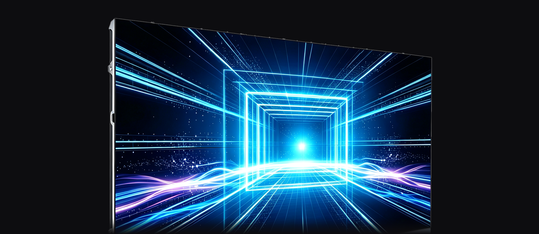
Against conventional SMD, COB raises emitting-chip density in the same area and pushes pixel pitch down to 0.4 mm and below: a clearer, smoother image, lower latency and better efficiency, which is what customers report back.
MIP development began in 2019. Through continued investment and iteration, yield and process capability have improved, Micro-level MIP has moved from breakthrough to volume production, and the products are entering the market. The range now sells domestically and exports to Europe, the Middle East, Southeast Asia and India, with the overseas share still rising.
Research and Standardisation
In Mini and Micro LED, intellectual property is the basis for competing globally. Research and development runs at 8 to 10% of revenue across the group’s technology arm.
AET also works with Peking University, Tsinghua University and French research institutes, and has established an academician workstation and a Guangdong doctoral workstation, focused on next-generation Micro LED materials, display chips and packaging processes.
Alongside its own development, AET works on standardisation. In 2024 it contributed to the industry’s first AM LED group standard, and it is promoting its fifth generation direct-view standard architecture — unifying size, resolution, mounting and interface so that products can move from commercial into consumer markets and widen the range of usable scenarios.
Visit or Audit the Plant
AET welcomes customer audits and factory visits at its Dongguan base. Contact the team to arrange a tour of the COB and MIP lines.
Related Articles & Insights
AET Opens Global Recruitment Across R&D, Sales and Service
AET has opened a global recruitment round covering display research, engineering, overseas sales and field service.
Five Extremes: How AET Plans to Grow
Minimalist architecture, frontier technology, visual quality, fine pitch and fast service: the five directions AET has organised i...