


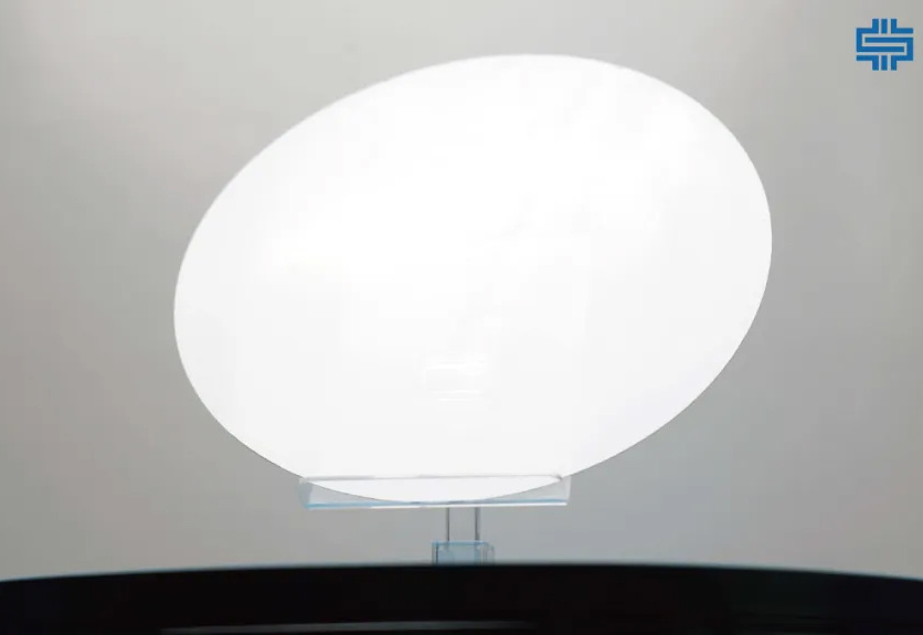
Dongguan China GaN Semiconductor Technology has announced a breakthrough in producing 6-inch and 8-inch free-standing gallium nitride single-crystal substrates, achieved on in-house ultra-large HVPE equipment.
The result fills a gap in HVPE-based 6 and 8-inch GaN substrate production internationally, and gives the domestic supply chain a position at the front of the technology.

Why GaN, and Why Wafer Size Matters
Gallium nitride is the representative material of the third generation of wide-bandgap semiconductors. Its wide bandgap, high breakdown field, high electron mobility and radiation tolerance make it important in consumer electronics, optoelectronics, power devices, communications and radar.
Homoepitaxy on a large substrate improves device performance further, which is why wafer diameter has become the constraint. Production GaN substrates have remained at 2 to 4 inches for two reasons: HVPE equipment for GaN crystal growth has generally supported only 2 to 4-inch wafers, and heterogeneous substrates such as sapphire and silicon introduce lattice mismatch and thermal expansion differences, leaving stress and warping that are hard to eliminate.
What Was Achieved
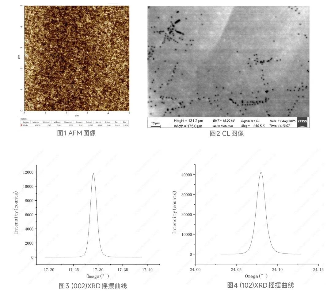
Using an in-house ultra-large HVPE reactor, the company solved the cracking and warping that limit large-diameter GaN growth, delivering a 6-inch substrate in early 2024 and then an 8-inch substrate, finished through grinding and coarse-to-fine polishing.
| Item | Detail |
|---|---|
| Substrate thickness | Over 450 µm |
| Surface roughness | Ra < 0.1 nm |
| Dislocation density | < 2E6 cm⁻² |
| FWHM | < 80 arcsec |
| Background carrier concentration | < 5E16 cm⁻³ |
| Electron mobility | > 800 cm²/(V·s) |
What It Changes for the Industry
-
Strategic Large-diameter GaN substrate technology has been dominated by Japanese suppliers. This result breaks that position and supports 8-inch GaN becoming an international process standard.
-
Compatibility An 8-inch GaN substrate fits existing 8-inch silicon-based production lines, shortening GaN-on-GaN development cycles and cutting the cost of converting a line.
-
Economics Larger wafers improve material utilisation and the number of chips per wafer, lowering unit cost and raising throughput.

The company was founded in January 2009 and is the Guangda Group’s principal industrial project in third-generation semiconductors.
The group’s layout covers substrate and epitaxy, chip process, packaging and end application. As the end-market brand, AET carries that coordinated capability into professional audiovisual solutions.
Substrate Supply and Partnership
Contact AET to discuss GaN substrate availability, specifications and joint development.
Related Articles & Insights
AET Opens Global Recruitment Across R&D, Sales and Service
AET has opened a global recruitment round covering display research, engineering, overseas sales and field service.
Five Extremes: How AET Plans to Grow
Minimalist architecture, frontier technology, visual quality, fine pitch and fast service: the five directions AET has organised i...